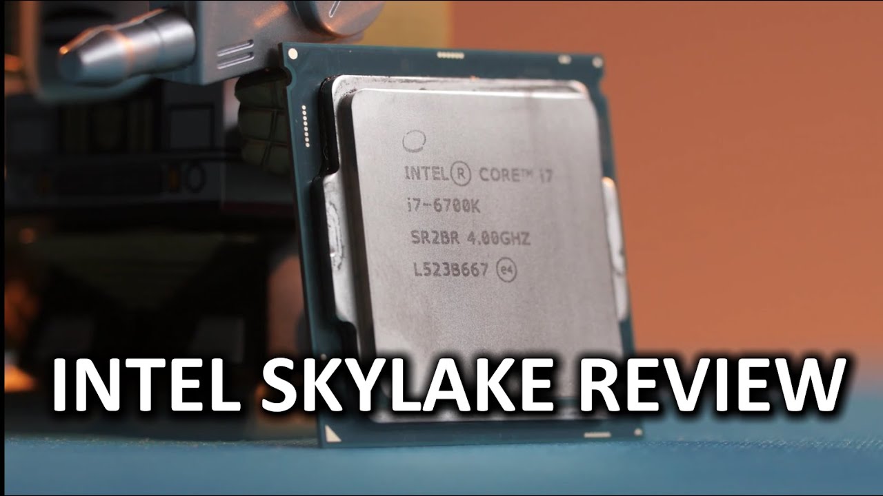
당신은 주제를 찾고 있습니까 “intel skylake – Intel 6700K \”Skylake\” CPU“? 다음 카테고리의 웹사이트 https://hu.taphoamini.com 에서 귀하의 모든 질문에 답변해 드립니다: https://hu.taphoamini.com/photos/. 바로 아래에서 답을 찾을 수 있습니다. 작성자 Linus Tech Tips 이(가) 작성한 기사에는 조회수 822,936회 및 좋아요 26,931개 개의 좋아요가 있습니다.
Table of Contents
intel skylake 주제에 대한 동영상 보기
여기에서 이 주제에 대한 비디오를 시청하십시오. 주의 깊게 살펴보고 읽고 있는 내용에 대한 피드백을 제공하세요!
d여기에서 Intel 6700K \”Skylake\” CPU – intel skylake 주제에 대한 세부정보를 참조하세요
Thanks to Braintree for supporting our channel. To learn more, and for your first $50,000 in transactions fee-free, go to http://www.braintreepayments.com/linus
Should you upgrade to a Z170 motherboard and a \”Skylake\” processor?
Logitech link: http://linustechtips.com/main/topic/322269-logitech-g303-daedalus-apex/
Pricing \u0026 discussion: http://linustechtips.com/main/topic/437130-intel-6700k/
Support us: http://linustechtips.com/main/topic/75969-support-linus-tech-tips-our-affiliates-and-sponsors/
Join our community forum: http://bit.ly/ZkLvE7
https://twitter.com/linustech
http://www.facebook.com/LinusTech
Intro Screen Music Credit:
Title: Laszlo – Supernova
Video Link: https://www.youtube.com/watch?v=PKfxmFU3lWY
iTunes Download Link: https://itunes.apple.com/us/album/supernova/id936805712
Artist Link: https://soundcloud.com/laszlomusic
Outro Screen Music Credit: Approaching Nirvana – Sugar High http://www.youtube.com/approachingnirvana
intel skylake 주제에 대한 자세한 내용은 여기를 참조하세요.
Chip Skylake là gì? Những điều cần biết về chip Skylate của …
Skylake là tên mã của Intel sử dụng cho một bộ vi xử lý được đưa ra vào tháng 8 năm 2015, sở hữu hiệu suất cao hơn so với người thừa kế …
Source: kimlongcenter.com
Date Published: 1/30/2022
View: 6730
Chip Skylake là gì? Lịch sử phát triển của chip Skylake
Skylake là một trong những dòng chip xử lý do Intel sản xuất và được tung ra thị trường vào cuối 2015. Đây là thế hệ tiếp theo của dòng chip …
Source: fptshop.com.vn
Date Published: 7/18/2022
View: 7620
Intel Skylake là gì? Bạn đã biết gì dòng chip thế hệ thứ 6 của …
Theo Intel, những gì họ làm để tạo ra vi xử lý Intel Skylake sẽ giúp cho CPU và GPU có được hiệu suất cao hơn. Cùng với đó là làm giảm tiêu thụ điện năng …
Source: viettelstore.vn
Date Published: 11/30/2021
View: 8600
Những điều cần biết về Skylake: phân loại, cải tiến về CPU và …
Skylake là thế hệ vi xử lý mới nhất của Intel và còn được gọi bằng cái tên Core thế hệ thứ 6. Đây sẽ là các CPU chủ đạo sắp xuất hiện trên rất nhiều máy …
Source: tinhte.vn
Date Published: 7/17/2021
View: 3451
Tìm hiểu Intel Core thế hệ thứ 6 Skylake: Có gì nổi bật? Có tốt …
Nếu bạn muốn tìm hiểu thêm những thông tin chi tiết về con chip Intel Core thế hệ thứ 6 Skylake thì đừng bỏ qua bài viết này để khám phá xem nó có gì nổi …
Source: www.thegioididong.com
Date Published: 5/27/2021
View: 1156
Skylake (microarchitecture) – Wikipedia
Skylake is a microarchitecture redesign using the same 14 nm manufacturing process technology as its predecessor, serving as a tock in Intel’s tick–tock …
Source: en.wikipedia.org
Date Published: 5/25/2022
View: 6047
주제와 관련된 이미지 intel skylake
주제와 관련된 더 많은 사진을 참조하십시오 Intel 6700K \”Skylake\” CPU. 댓글에서 더 많은 관련 이미지를 보거나 필요한 경우 더 많은 관련 기사를 볼 수 있습니다.
주제에 대한 기사 평가 intel skylake
- Author: Linus Tech Tips
- Views: 조회수 822,936회
- Likes: 좋아요 26,931개
- Date Published: 2015. 8. 25.
- Video Url link: https://www.youtube.com/watch?v=fQ63w5_vXbg
Skylake (microarchitecture)
CPU microarchitecture by Intel
Skylake[6][7] is the codename used by Intel for a processor microarchitecture that was launched in August 2015[8] succeeding the Broadwell microarchitecture.[9] Skylake is a microarchitecture redesign using the same 14 nm manufacturing process technology[10] as its predecessor, serving as a tock in Intel’s tick–tock manufacturing and design model. According to Intel, the redesign brings greater CPU and GPU performance and reduced power consumption. Skylake CPUs share their microarchitecture with Kaby Lake, Coffee Lake, Cannon Lake, Whiskey Lake, and Comet Lake CPUs.
Skylake is the last Intel platform on which Windows earlier than Windows 10 will be officially supported by Microsoft,[11] although enthusiast-created modifications exist that allow Windows 8.1 and earlier to continue to receive Windows Updates on later platforms.[12][13][14]
Some of the processors based on the Skylake microarchitecture are marketed as 6th-generation Core.[15][16][17]
Intel officially declared end of life and discontinued Skylake LGA 1151 CPUs on March 4, 2019.[18]
Development history [ edit ]
Skylake’s development, as with previous processors such as Banias, Dothan, Conroe, Sandy Bridge, and Ivy Bridge, was primarily undertaken by Intel Israel at its engineering research center in Haifa, Israel.[19] The final design was largely an evolution of Haswell, with minor improvements to performance and several power-saving features being added.[20] A major priority of Skylake’s design was to design a microarchitecture for envelopes as low as 4.5W to embed within tablet computers and notebooks in addition to higher-power desktop computers and servers.[21]
In September 2014, Intel announced the Skylake microarchitecture at the Intel Developer Forum in San Francisco, and that volume shipments of Skylake CPUs were scheduled for the second half of 2015. The Skylake development platform was announced to be available in Q1 2015. During the announcement, Intel also demonstrated two computers with desktop and mobile Skylake prototypes: the first was a desktop testbed system, running the latest version of 3DMark, while the second computer was a fully functional laptop, playing 4K video.[22]
An initial batch of Skylake CPU models (6600K and 6700K) was announced for immediate availability during the Gamescom on August 5, 2015,[23] unusually soon after the release of its predecessor, Broadwell, which had suffered from launch delays.[24] Intel acknowledged in 2014 that moving from 22 nm (Haswell) to 14 nm (Broadwell) had been its most difficult process to develop yet, causing Broadwell’s planned launch to slip by several months;[25] yet, the 14 nm production was back on track and in full production as of Q3 2014.[26] Industry observers had initially believed that the issues affecting Broadwell would also cause Skylake to slip to 2016, but Intel was able to bring forward Skylake’s release and shorten Broadwell’s release cycle instead.[27][28] As a result, the Broadwell architecture had an unusually short run.[27]
Overclocking of unsupported processors [ edit ]
Officially Intel supported overclocking of only the K and X versions of Skylake processors. However, it was later discovered that other non-K chips could be overclocked by modifying the base clock value – a process made feasible by the base clock applying only to the CPU, RAM, and integrated graphics on Skylake. Through beta UEFI firmware updates, some motherboard vendors, such as ASRock (which prominently promoted it under the name Sky OC) allowed the base clock to be modified in this manner.[29][30]
When overclocking unsupported processors using these UEFI firmware updates, several issues arise:
C-states are disabled, therefore the CPU will constantly run at its highest frequency and voltage
Turbo-boost is disabled
Integrated graphics are disabled
AVX2 instruction performance is poor, approximately 4-5 times slower due to the upper 128-bit half of the execution units and data buses not being taken out of their power saving states
CPU core temperature readings are incorrect
These issues are partly caused by the power management of the processor needing to be disabled for base clock overclocking to work.[31]
In February 2016, however, an ASRock firmware update removed the feature. On February 9, 2016, Intel announced that it would no longer allow such overclocking of non-K processors, and that it had issued a CPU microcode update that removes the function.[32][33][34] In April 2016, ASRock started selling motherboards that allow overclocking of unsupported CPUs using an external clock generator.[35][36]
Operating system support [ edit ]
In January 2016, Microsoft announced that it would end support of Windows 7 and Windows 8.1 on Skylake processors effective July 17, 2017; after this date, only the most critical updates for the two operating systems would be released for Skylake users if they have been judged not to affect the reliability of the OS on older hardware, and Windows 10 would be the only Microsoft Windows platform officially supported on Skylake, as well as all future Intel CPU microarchitectures beginning with Skylake’s successor Kaby Lake. Terry Myerson stated that Microsoft had to make a large investment in order to reliably support Skylake on older versions of Windows, and that future generations of processors would require further investments. Microsoft also stated that due to the age of the platform, it would be challenging for newer hardware, firmware, and device driver combinations to properly run under Windows 7.[37][38]
On March 18, 2016, in response to criticism over the move, primarily from enterprise customers, Microsoft announced revisions to the support policy, changing the cutoff for support and non-critical updates to July 17, 2018 and stating that Skylake users would receive all critical security updates for Windows 7 and 8.1 through the end of extended support.[39][40] In August 2016, citing “a strong partnership with our OEM partners and Intel”, Microsoft stated that it would continue to fully support 7 and 8.1 on Skylake through the end of their respective lifecycles.[41][42] In addition, an enthusiast-created modification was released that disabled the Windows Update check and allowed Windows 8.1 and earlier to continue to be updated on this and later platforms.[43]
As of Linux kernel 4.10, Skylake mobile power management is supported with most Package C states supported seeing some use. Linux 4.11 enables Frame-Buffer Compression for the integrated graphics chipset by default, which lowers power consumption.[44]
Skylake is fully supported on OpenBSD 6.2 and later, including accelerated graphics.[45]
For Windows 11, only the high-end Skylake-X processors are officially listed as compatible.[46] All other Skylake processors are not officially supported due to security concerns.[47] However, it is still possible to manually upgrade using an ISO image (as Windows 10 users on those processors won’t be offered to upgrade to Windows 11 via Windows Update), or perform a clean installation as long as the system has Trusted Platform Module (TPM) 2.0 enabled,[48] but the user must accept that they will not be entitled to receive updates, and that damage caused by using Windows 11 on an unsupported configuration are not covered by the manufacturer’s warranty.[49][50]
Features [ edit ]
Skylake i7-6700K: Top view
Skylake i7-6700K: Bottom view
Like its predecessor, Broadwell, Skylake is available in five variants, identified by the suffixes S (SKL-S), X (SKL-X), H (SKL-H), U (SKL-U), and Y (SKL-Y). SKL-S and SKL-X contain overclockable K and X variants with unlocked multipliers.[51] The H, U and Y variants are manufactured in ball grid array (BGA) packaging, while the S and X variants are manufactured in land grid array (LGA) packaging using a new socket, LGA 1151 (LGA 2066 for Skylake X).[52] Skylake is used in conjunction with Intel 100 Series chipsets, also known as Sunrise Point.[53]
The major changes between the Haswell and Skylake architectures include the removal of the fully integrated voltage regulator (FIVR) introduced with Haswell.[54] On the variants that will use a discrete Platform Controller Hub (PCH), Direct Media Interface (DMI) 2.0 is replaced by DMI 3.0, which allows speeds of up to 8 GT/s.
Skylake’s U and Y variants support one DIMM slot per channel, while H and S variants support two DIMM slots per channel.[52] Skylake’s launch and sales lifespan occur at the same time as the ongoing SDRAM market transition, with DDR3 SDRAM memory gradually being replaced by DDR4 memory. Rather than working exclusively with DDR4, the Skylake microarchitecture remains backward compatible by interoperating with both types of memory. Accompanying the microarchitecture’s support for both memory standards, a new SO-DIMM type capable of carrying either DDR3 or DDR4 memory chips, called UniDIMM, was also announced.[55]
Skylake’s few P variants have a reduced on-die graphics unit (12 execution units enabled instead of 24 execution units) over their direct counterparts; see the table below. In contrast, with Ivy Bridge CPUs the P suffix was used for CPUs with completely disabled on-die video chipset.
Other enhancements include Thunderbolt 3.0, SATA Express, Iris Pro graphics with Direct3D feature level 12_1 with up to 128 MB of L4 eDRAM cache on certain SKUs.[56] The Skylake line of processors retires VGA support,[57] while supporting up to five monitors connected via HDMI 1.4, DisplayPort 1.2 or Embedded DisplayPort (eDP) interfaces.[58] HDMI 2.0 (4K@60 Hz) is only supported on motherboards equipped with Intel’s Alpine Ridge Thunderbolt controller.[59]
The Skylake instruction set changes include Intel MPX (Memory Protection Extensions) and Intel SGX (Software Guard Extensions). Future Xeon variants will also have Advanced Vector Extensions 3.2 (AVX-512F).[3][4]
Skylake-based laptops were predicted to use wireless technology called Rezence for charging, and other wireless technologies for communication with peripherals. Many major PC vendors agreed to use this technology in Skylake-based laptops; however, no laptops were released with the technology as of 2019.[60][61]
The integrated GPU of Skylake’s S variant supports on Windows DirectX 12 Feature Level 12_1, OpenGL 4.6 with latest Windows 10 driver update[62] (OpenGL 4.5 on Linux[63]) and OpenCL 3.0 standards. The Quick Sync video engine now includes support for VP9 (GPU accelerated decode only), VP8 and HEVC (hardware accelerated 8-bit encode/decode and GPU accelerated 10-bit decode), and supports for resolutions up to 4096 × 2048.[64][65][66]
Intel also released unlocked (capable of overclocking) mobile Skylake CPUs.[67]
Unlike previous generations, Skylake-based Xeon E3 no longer works with a desktop chipset that supports the same socket, and requires either the C232 or the C236 chipset to operate.
Known issues [ edit ]
Short loops with a specific combination of instruction use may cause unpredictable system behavior on CPUs with hyperthreading. A microcode update was issued to fix the issue.[68]
Skylake is vulnerable to Spectre attacks.[69] In fact, it is more vulnerable than other processors because it uses indirect branch speculation not just on indirect branches but also when the return prediction stack underflows.
The latency for the spinlock PAUSE instruction has been increased dramatically (from the usual 10 cycles to 141 cycles in Skylake), which can cause performance issues with older programs or libraries using pause instructions.[70] Intel documents the increased latency as a feature that improves power efficiency.[71]
Architecture changes compared to Broadwell microarchitecture [ edit ]
CPU [ edit ]
GPU [ edit ]
Other [ edit ]
Configurations [ edit ]
Skylake processors are produced in five main families: Y, U, H, S, and X. Multiple configurations are available within each family:[52]
Feature Family Y U H T S R X W SP Integrated L4 cache • • • Low-power mobile/embedded systems • • • • Socket BGA LGA 1151 LGA 2066 LGA 3647 DDR3L SDRAM • • • • • • DDR4 SDRAM • • • • • • • 128 GB (GB) of physical RAM • • •+ 28 to 44 PCIe 3.0 lanes
• • •
List of Skylake processor models [ edit ]
Mainstream desktop processors [ edit ]
Intel i7-6700 die shot
Common features of the mainstream desktop Skylake CPUs:
DMI 3.0 and PCIe 3.0 interfaces
Dual channel memory support in the following configurations: DDR3L-1600 1.35 V (32 GB maximum) or DDR4-2133 1.2 V (64 GB maximum). DDR3 is unofficially supported through some motherboard vendors [89] [90] [91]
16 PCI-E 3.0 lanes
The Core-branded processors support the AVX2 instruction set. The Celeron and Pentium-branded ones support only SSE4.1/4.2
350 MHz base graphics clock rate
High-end desktop processors (Skylake-X) [ edit ]
Common features of the high performance Skylake-X CPUs:
Quad channel memory support for DDR4-2400 (on the i7-7800X) or DDR4-2666 (on all other CPUs) [93] up to 128 GB
up to 128 GB 28 (for the i7-7800X and i7-7820X) to 44 (for all other CPUs) PCI-E 3.0 lanes
In addition to the AVX2 instruction set, they also support the AVX-512 instructions
No built-in iGPU (integrated graphics processor)
Turbo Boost Max Technology 3.0 for up to 2/4 threads workloads for CPUs that have 8 cores and more (7820X, 7900X, 7920X, 7940X, 7960X, 7980XE, and all 9th generation chips) [94]
A different cache hierarchy (when compared to client Skylake CPUs or previous architectures)
Intel i7-7820X die shot
7th generation Skylake-X high-end desktop CPUs Cores
(threads) Processor
branding and model CPU
clock
rate Turbo clock GHz L2
cache L3
cache TDP Socket Release
date Release
price
(USD) TB 2.0 TB Max 3.0 18 (36) Core i9 [95] 7980XE 2.6 GHz 4.2 4.4 1 MB
per
core 1 ⅜ MB
per
core 165 W LGA 2066 September 25,
2017[96] $1999 16 (32) 7960X 2.8 GHz $1699 14 (28) 7940X 3.1 GHz 4.3 $1399 12 (24) 7920X 2.9 GHz 140 W August 28, 2017 $1189 10 (20) 7900X 3.3 GHz 4.5 June 19, 2017 $999 8 (16) Core i7 7820X 3.6 GHz $599 6 (12) 7800X 3.5 GHz 4.0 — $389
9th generation Skylake-X high-end desktop CPUs Cores
(threads) Processor
branding and model CPU
clock
rate Turbo clock GHz L2
cache L3
cache TDP Socket Release
date Release
price
(USD) TB 2.0 TB Max 3.0 14 (28) Core i9 [97] 9990XE[98] 4.0 GHz 5.0 5.0 1 MB
per
core 19.25 MB 255 W LGA 2066 January 3, 2019 OEM only 18 (36) 9980XE 3.0 GHz 4.4 4.5 24.75 MB 165 W October 9, 2018[99] $1979 16 (32) 9960X 3.1 GHz 22 MB $1684 14 (28) 9940X 3.3 GHz 19.25 MB $1387 12 (24) 9920X 3.5 GHz $1189 10 (20) 9900X 3.5 GHz $989 9820X 3.3 GHz 4.1 4.2 16.5 MB $889 8 (16) Core i7 9800X 3.8 GHz[100] 4.4 4.5 $589
Xeon High-end desktop processors (Skylake-X) [ edit ]
Is Xeon instead of Core
Uses C621 Chipset
Xeon W-3175X is the only Xeon with a multiplier unlocked for overclocking
Model
number sSpec
number Cores
(threads) Frequency Turbo Boost
all-core/2.0
(/max. 3.0) L2
cache L3
cache TDP Socket I/O bus Memory Release date Part
number(s) Release
price (USD) Xeon W-3175X SRF6L (H0) 28 (56) 3.1 GHz 3.8/4.3 GHz 28 × 1 MB 38.50 MB 255 W LGA 3647 DMI 3.0 6 × DDR4-2666 January 30, 2019 CD8067304237800
BX80673W3175X $2999
Mobile processors [ edit ]
See also Server, Mobile below for mobile workstation processors.
Target
segment Cores
(threads) Processor
branding and
model CPU
clock
rate CPU Turbo clock rate GPU GPU clock rate L3
cache L4
cache Max.
PCIe
lanes TDP cTDP Release date Price (USD) Single
core Dual
core Quad
core Base Max Up Down Performance 4 (8) Core i7 6970HQ 2.8 GHz 3.7 GHz ? Iris Pro 580 350 MHz 1050 MHz 8 MB 128 MB 16 45 W — 35 W Q1 2016 $623 6920HQ 2.9 GHz 3.8 GHz 3.6 GHz 3.4 GHz HD 530 — September 1, 2015 $568 6870HQ 2.7 GHz 3.6 GHz ? Iris Pro 580 1000 MHz 128 MB Q1 2016 $434 6820HQ 3.4 GHz 3.2 GHz HD 530 1050 MHz — September 1, 2015 $378 6820HK 6770HQ 2.6 GHz 3.5 GHz ? Iris Pro 580 950 MHz 6 MB 128 MB Q1 2016 $434 6700HQ 3.3 GHz 3.1 GHz HD 530 1050 MHz — September 1, 2015 $378 Mainstream 2 (4) 6660U 2.4 GHz 3.4 GHz 3.2 GHz — Iris 540 300 MHz 4 MB 64 MB 12 15 W 9.5 W Q1 2016 $415 6650U 2.2 GHz Q3 2015 6600U 2.6 GHz — HD 520 — 25 W 7.5 W September 1, 2015 $393 6567U 3.3 GHz 3.6 GHz 3.4 GHz Iris 550 1100 MHz 64 MB 28 W — 23 W Q3 2015 TBD 6560U 2.2 GHz 3.2 GHz 3.1 GHz Iris 540 1050 MHz 15 W 9.5 W 6500U 2.5 GHz 3.1 GHz 3.0 GHz HD 520 — 7.5 W September 1, 2015 $393 4 (4) Core i5 6440HQ 2.6 GHz 3.5 GHz 3.3 GHz 3.1 GHz HD 530 350 MHz 950 MHz 6 MB 16 45 W 35 W $250 2 (4) 6360U 2.0 GHz 3.1 GHz 2.9 GHz — Iris 540 300 MHz 1000 MHz 4 MB 64 MB 12 15 W 9.5 W Q3 2015 $304 4 (4) 6350HQ 2.3 GHz 3.2 GHz ? Iris Pro 580 350 MHz 900 MHz 6 MB 128 MB 16 45 W 35 W Q1 2016 $306 6300HQ 3.0 GHz 2.8 GHz HD 530 950 MHz — September 1, 2015 $250 2 (4) 6300U 2.4 GHz 3.0 GHz 2.9 GHz — HD 520 300 MHz 1000 MHz 3 MB 12 15 W 7.5 W $281 6287U 3.1 GHz 3.5 GHz 3.3 GHz Iris 550 1100 MHz 4 MB 64 MB 28 W 23 W Q3 2015 $304 6267U 2.9 GHz 3.3 GHz 3.1 GHz 1050 MHz 23 W 6260U 1.8 GHz 2.9 GHz 2.7 GHz Iris 540 950 MHz 15 W 9.5 W $304 6200U 2.3 GHz 2.8 GHz HD 520 1000 MHz 3 MB — 7.5 W September 1, 2015 $281 Core i3 6167U 2.7 GHz — — Iris 550 64 MB 28 W 23 W Q3 2015 $304 6157U 2.4 GHz Q3 2016 6100H 2.7 GHz HD 530 350 MHz 900 MHz — 35 W — September 1, 2015 $225 6100U 2.3 GHz HD 520 300 MHz 1000 MHz 15 W 7.5 W $281 6006U 2.0 GHz 900 MHz — November, 2016 $281 Core m7 6Y75 1.2 GHz 3.1 GHz 2.9 GHz HD 515 300 MHz 1000 MHz 4 MB 10 4.5 W 7 W 3.5 W September 1, 2015 $393 Core m5 6Y57 1.1 GHz 2.8 GHz 2.4 GHz 900 MHz $281 6Y54 2.7 GHz Core m3 6Y30 0.9 GHz 2.2 GHz 2.0 GHz 850 MHz 3.8 W Pentium 4405U 2.1 GHz — — HD 510 950 MHz 2 MB 15 W — 10 W Q3 2015 $161 4405Y 1.5 GHz HD 515 800 MHz 6 W 4.5 W 2 (2) Celeron G3902E 1.6 GHz — HD 510 350 MHz 950 MHz 16 25 W — Q1 2016 $107 G3900E 2.4 GHz 35 W 3955U 2.0 GHz 300 MHz 900 MHz 10 15 W 10 W Q4 2015 3855U 1.6 GHz
Workstation processors [ edit ]
Server processors [ edit ]
E3 series server chips all consist of System Bus 9 GT/s, max. memory bandwidth of 34.1 GB/s dual channel memory. Unlike its predecessor, the Skylake Xeon CPUs require C230 series (C232/C236) or C240 series (C242/C246) chipset to operate, with integrated graphics working only with C236 and C246 chipsets. Mobile counterparts uses CM230 and CM240 series chipsets.
Skylake-SP (14 nm) Scalable Performance [ edit ]
Xeon Platinum supports up to 8 sockets. Xeon Gold supports up to 4 sockets. Xeon Silver and Bronze support up to 2 sockets. −M: 1536 GB RAM per socket instead of 768 GB RAM for non −M SKUs −F: integrated OmniPath fabric −T: High thermal-case and extended reliability
Support for up to 12 DIMMs of DDR4 memory per CPU socket.
Xeon Platinum, Gold 61XX, and Gold 5122 have two AVX-512 FMA units per core. Xeon Gold 51XX (except 5122), Silver, and Bronze have a single AVX-512 FMA unit per core.
Xeon Bronze and Silver (dual processor) [ edit ]
Xeon Bronze 31XX has no HT or Turbo Boost support.
Xeon Bronze 31XX supports DDR4-2133 MHz RAM. Xeon Silver 41XX supports DDR4-2400 MHz RAM.
Xeon Bronze 31XX and Xeon Silver 41XX support two UPI links at 9.6 GT/s.
Xeon Gold (quad processor) [ edit ]
Xeon Gold 51XX and F SKUs has two UPIs at 10.4 GT/s. Xeon Gold 61XX has three UPIs at 10.4 GT/s.
Xeon Gold 51XX support DDR4-2400 MHz RAM (except 5122). Xeon Gold 5122 and 61XX support DDR4-2666 MHz RAM.
Intel Skylake Xeon gold processor
Intel Skylake Xeon gold processor, delidded
Die shot
Xeon Platinum (octal processor) [ edit ]
Xeon Platinum non-F SKUs have three UPIs at 10.4 GT/s. Xeon Platinum F-SKUs have two UPIs at 10.4 GT/s.
Xeon Platinum supports DDR4-2666 MHz RAM.
See also [ edit ]
키워드에 대한 정보 intel skylake
다음은 Bing에서 intel skylake 주제에 대한 검색 결과입니다. 필요한 경우 더 읽을 수 있습니다.
이 기사는 인터넷의 다양한 출처에서 편집되었습니다. 이 기사가 유용했기를 바랍니다. 이 기사가 유용하다고 생각되면 공유하십시오. 매우 감사합니다!
사람들이 주제에 대해 자주 검색하는 키워드 Intel 6700K \”Skylake\” CPU
- intel
- 6700k
- skylake
- cpu
- review
- unboxing
- overview
- testing
- benchmark
- overclocking
- gaming
- graphics
- processor
Intel #6700K #\”Skylake\” #CPU
YouTube에서 intel skylake 주제의 다른 동영상 보기
주제에 대한 기사를 시청해 주셔서 감사합니다 Intel 6700K \”Skylake\” CPU | intel skylake, 이 기사가 유용하다고 생각되면 공유하십시오, 매우 감사합니다.